| V.35
M34 connector to DB25 connector |
|
|
V.35 Cable Interface |
V.35 cable & M/34 to M/34 and V.35-M/34 cable to DB25
jump to - V.35, RS422, RS530 to HSSI
CONVETER
jump to -
V.35 to RS232 Mini CONVETER
ARC Electronics
jump to ... Home Page
The Faster Serial Interface.
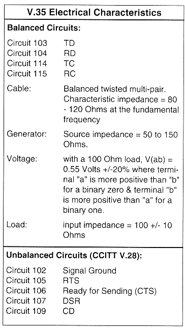
Basically, V.35 is a high-speed serial interface designed to support both higher data rates and connectivity between DTEs (data-terminal equipment) or DCEs (data-communication equipment) over digital lines.
V.35 is an interface (V.35 is the ITU - formerly CCITT standard termed "Data Transmission at 48 Kbps Using 60-108 KHz Group-Band Circuits") commonly used on higher speed circuits of 56kbps and above. Recognizable by its blocky, 34-pin connector; V.35 combines the bandwidth of several telephone circuits to provide the high-speed interface between a DTE or DCE and a CSU/DSU (Channel Service Unit/Data Service Unit). To achieve such high speeds and great distances, V.35 combines both balanced and unbalanced voltage signals on the same interface. Transmission is usually a synchronous protocol (note clocking pins i.e. receive and transmit clock). Although V.35 is commonly used to support speeds ranging anywhere from 48 to 64 Kbps, much higher rates are possible [ ISDN (64 or 128Kbps), Factional T1@ 128 Kbps to 1.544Mbps T1, ATM and Frame Relay]. V.35 cable distances theoretically can range up to 4000 feet (1200 m) at speeds up to 100 Kbps. Actual distances will depend on your equipment and the quality of the cable . Lan routers often come equipped with a V.35 electrical interface but many today are using a HSSI interface at speeds higher than T1 and above (typical T3 45Mbps).
| V.35
M34 connector to DB25 connector |
|
|
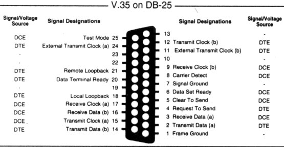
jump to V.35 on a DB25 used by some manufactures
V.35 cable cross-over for tail circuits
| V.35 cable cross-over for tail circuits | 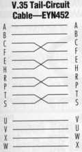 |
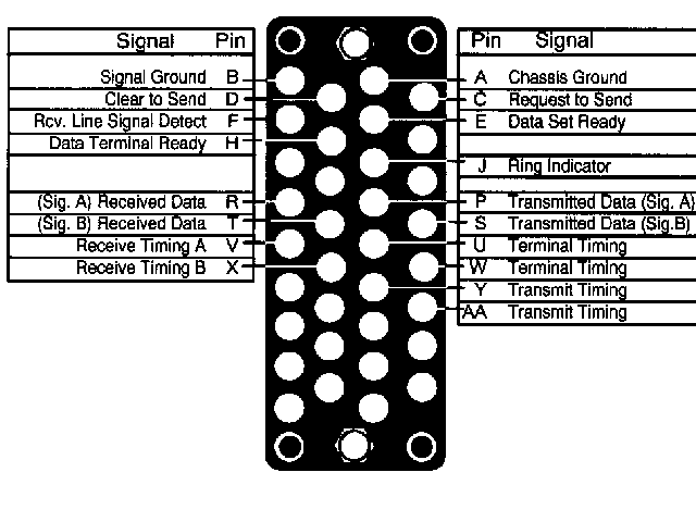
V.35 cable 18 pin layout
V.35 cable Pin # Source
Description
* indicates if source is DTE or DCE
| A - Common Chassis Ground B - Common Signal Ground C - * DTE Request to Send D - * DCE "CTS" Clear to Send E - * DCE "DSR" Data Set Ready F - * DCE "DCD" Data Carrier Detect H - * DTE "DTR" Data Terminal Ready J - * DCE "RI" Ring Indicator K - Local Test L - Unassigned M - Unassigned N - Unassigned P - * DTE "SD" Send Data A Balanced R - * DCE "RD" Receive Data A Balanced S - * DTE "SD" Send Data B Balanced T - * DCE "RD" Receive Data B Balanced U - * DTE Terminal Timing A Balanced |
V - *
DCE Receive Timing A Balanced W - * DTE Terminal Timing B Balanced X - * DCE Receive Timing B Balanced Y - * DCE Send Timing A Balanced Z - Unassigned AA - * DCE Send Timing B Balanced BB - Unassigned CC - Unassigned DD - Unassigned EE - Unassigned FF - Unassigned HH - Unassigned JJ - Unassigned KK - Unassigned LL - Unassigned MM - Unassigned NN - Unassigned |
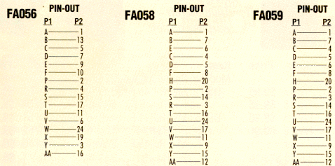
V.35 cable Connector pin layout